
How a Chip Is Made

In this Interest


How a Chip Is Made
Snapshot
A microchip is a silicon crystal built up in layers: a wafer is grown, sliced and polished, then patterned, etched, doped and wired over hundreds of steps before it is tested and cut apart.
The work happens at dimensions below 20 nanometres, which is why so few companies can do it at all.
By the end you will be able to say what each step does, which machine sets the limit, and where the supply chain narrows to one or two firms.
This brief runs about ten minutes.

How a Chip Is Made
Why Now
On 8 April 2026 the Semiconductor Equipment Association of Japan reported that worldwide billings of chipmaking equipment reached 135.1 billion dollars in 2025, up 15 per cent on 2024. China, Taiwan and South Korea billed 106.6 billion of that total, 79 per cent of the market. The same release records where the growth came from: Taiwan up 90 per cent to 31.5 billion dollars on advanced logic capacity, Korea up 26 per cent on memory. Europe fell 41 per cent to 2.9 billion dollars.
The equipment itself is moving faster than the money. ASML states that its EXE platform, the High-NA generation with a numerical aperture of 0.55, supports high-volume manufacturing in 2025 and 2026, starting at the 2 nm logic node and printing at a resolution of 8 nm. The NXE generation it extends has printed 13 nm features at 0.33 since the 7 nm, 5 nm and 3 nm nodes.
What changed is the resolution and the number of steps that can be removed. What did not change is the physics: the industry still exposes with 13.5 nm light, still needs a vacuum, and still has one supplier of the scanners.
How a Chip Is Made
The Explainer
From Quartz to a Single Crystal
Silicon starts as quartz, reduced with carbon in an electric furnace. The result is metallurgical grade silicon, about 98 to 99 per cent pure, with iron, aluminium, boron and phosphorus still in it. That is far too dirty for a transistor.
The purification is chemical rather than physical. Crushed metallurgical silicon reacts with hydrogen chloride to form trichlorosilane, a liquid that boils at 31.8 degrees Celsius. Because the impurity chlorides boil at different temperatures, fractional distillation separates them, and the trichlorosilane that leaves the columns is clean to parts per billion. It is then mixed with hydrogen and passed over silicon filaments heated to up to 1,150 degrees Celsius, where it decomposes and deposits silicon. Electronic grade polysilicon is quoted at 10N to 11N, which is 99.99999999 per cent pure or better.
The crystal comes next. In the Czochralski process a seed crystal is dipped into molten silicon and pulled slowly upward while rotating, so the atoms lock onto the seed orientation and the whole ingot is one crystal with no grain boundaries. The ingot is ground to a diameter of 300 millimetres, sliced into wafers 775 micrometres thick, lapped and polished to a mirror.
The Pattern and the Light
Every layer begins with a pattern. The wafer is coated with a photoresist, a polymer that changes solubility when light strikes it. A mask carries the pattern for one layer, the resist is exposed through it, and the exposed or unexposed regions are washed away. What remains is a stencil.
For two decades the light was 193 nm from an argon fluoride laser, and the industry kept printing smaller features by splitting one layer into several exposures, correcting the mask for diffraction, and putting water between the lens and the wafer. The cost is visible in the count: IEEE Spectrum reported in 2018 that the most complex processors needed about 80 trips through the lithography tool. GlobalFoundries planned to replace 15 steps with 5 at 7 nm by using EUV. Without it, its chief technology officer said, a 5 nm process would need more than 100 lithographic steps.
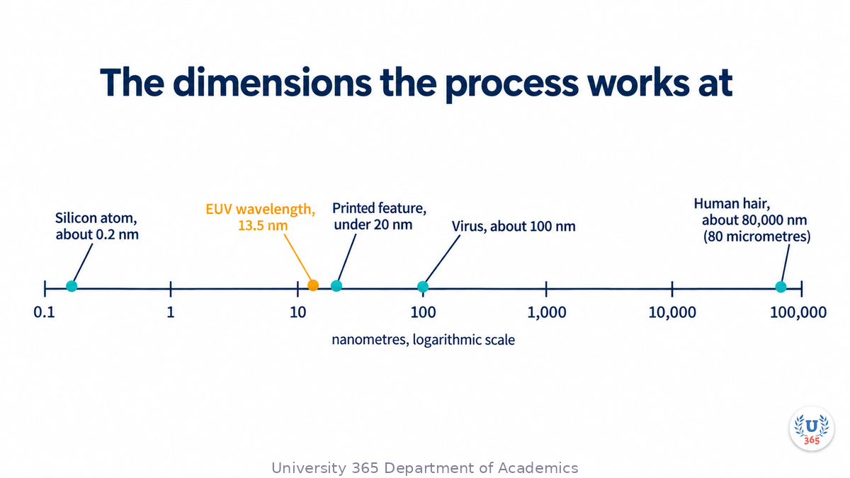
EUV changes the light, not the idea. The wavelength is 13.5 nm, which is absorbed by air, by glass and by every lens material, so the whole optical path sits in a vacuum and the image is formed by mirrors. The light comes from tin. ZEISS describes the source: 50,000 droplets of molten tin are fired into a vacuum chamber every second and struck by two pulses from a 30 kilowatt carbon dioxide laser. The first pulse flattens each droplet, the second turns it into a plasma at nearly 220,000 degrees Celsius, close to 40 times the surface temperature of the sun. The plasma radiates at 13.5 nm.
The mirrors are the precision problem in one object. Each is a curved substrate with a multilayer coating, and the figure error is measured in fractions of a nanometre. ZEISS puts it in a form you can hold: enlarge one mirror to the size of Germany and the largest unevenness would be 0.1 millimetres high. ASML invested more than 6 billion euros in EUV research over 17 years and bought Cymer for the light source; it is the only company selling EUV scanners for production.
Etch, Deposit, Dope
Once the resist stencil exists, the pattern has to move into the material. Plasma etching does that: a radio frequency field ionises a gas, ions are accelerated toward the wafer and remove material where the resist is open, while the sidewalls are passivated so the cut stays vertical. A layer that needs a hard mask gets one, because resist alone erodes.
Adding material is the other half. Chemical vapour deposition flows a gas that reacts at the surface and leaves a film. Physical vapour deposition sputters a target and condenses the metal. Atomic layer deposition goes further: each cycle reacts one precursor with the surface until every site is consumed, purges, then introduces the second. The reaction stops when the surface is saturated, so the film grows one atomic layer per cycle, which is why a gate dielectric a few nanometres thick stays uniform across a 300 mm wafer.
Doping sets the electrical behaviour. An ion implanter ionises the dopant, accelerates it to a chosen energy and fires it into the silicon. An anneal afterwards repairs the crystal damage and puts the dopant atoms on lattice sites where they donate or accept electrons.
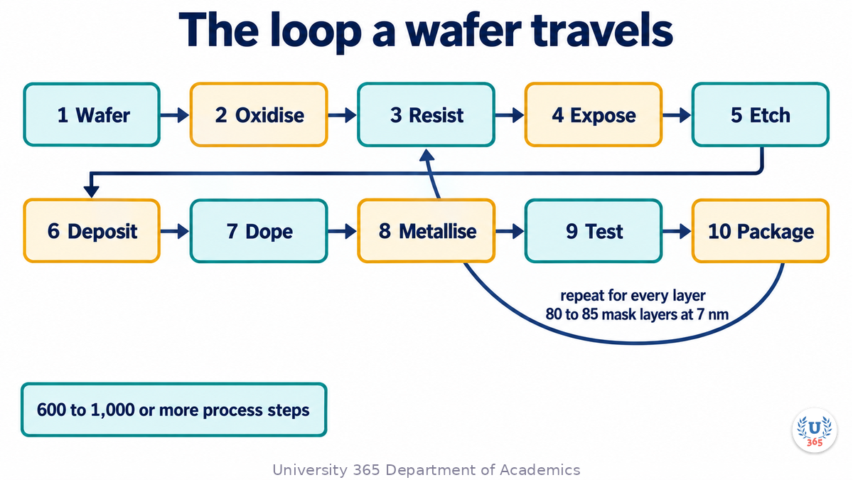
Then the loop repeats. Semiconductor Engineering reports that an advanced logic process runs 600 to 1,000 steps or more, and that mask layers rise from 40 to 50 at 28 nm to 60 at 14 and 10 nm, 80 to 85 at 7 nm, and possibly 100 at 5 nm. A fab takes one to one and a half days per mask layer, so the calendar follows the layer count.
Wiring, Test and Package
The transistors are only half the chip. The connections between them are built in the back end, and they became the harder problem: at 0.25 micrometres the resistance and capacitance of the wiring began to dominate the delay of the circuit, which is why the industry changed both materials.
Aluminium was replaced by copper, which conducts better: 1.678 against 2.65 microhm centimetres. Copper cannot be patterned by etching, because its chlorides and fluorides are not volatile enough to leave the wafer. So the process was inverted. Trenches and vias are etched into the dielectric first, a tantalum nitride and tantalum barrier is sputtered to stop copper diffusing into the insulator, a thin copper seed is sputtered, and copper is electroplated into the features. The plating bath is engineered so deposition is suppressed at the top of a trench and accelerated at the bottom, which fills the feature from the base upward without a void. Chemical mechanical polishing then removes the overburden and leaves copper only in the trenches. The sequence is the dual damascene process, and the dielectric around it is a low-k material chosen to reduce capacitance.
What leaves the fab is a wafer covered in identical dice that have never been separated or powered as a product. A probe station touches each die and runs a test program, and the failing dice are marked. Good dice are cut out, attached to a package substrate, connected by wire bonds or flip-chip bumps, encapsulated and tested again. Advanced packaging now carries part of the performance story, and the SEAJ data shows test equipment billings up 55 per cent and assembly and packaging equipment up 21 per cent in 2025, against 12 per cent for wafer processing.
How a Chip Is Made
The Feynman Summary
Here is the whole thing without the vocabulary. You start with sand, which is silicon dioxide. You heat it with carbon to get silicon, but that silicon is only about 99 per cent pure. So you turn it into a liquid chemical, distil it until the impurities are gone, and turn it back into solid silicon. You melt that silicon, dip in a small crystal and pull it up slowly, and the whole ingot copies that crystal's atomic arrangement. You slice the ingot into wafers.
Then you build the chip the way you would print and etch a stack of stencils. Coat the wafer with a light sensitive plastic, shine a pattern onto it, wash away the soft parts, and use what remains to protect the wafer while plasma cuts the pattern into the layer below. Add a new layer of material, and do it again. Dope the silicon in chosen places so it conducts the way you want, then build metal wires between the parts.
Every layer is the same cycle, and a modern chip runs it eighty times or more. When the wafer is finished you test each die on it, cut the die out, put it in a package and test it again.
How a Chip Is Made
The Evidence
The evidence for this process is unusually good, because most of it is written down by the people who run it. The tool specifications come from the manufacturers: ASML states the wavelength, the numerical aperture, the resolution and the research spend, and ZEISS states the source parameters and the mirror tolerance. The IEEE Spectrum report from January 2018 supplies the step counts that make the economics legible.
The money is measured by industry associations rather than estimated by a journalist. SEAJ collects monthly billings from more than 95 equipment companies jointly with SEMI, and its April 2026 release gives the regional totals, the year on year changes and the 135.06 billion dollar total. The mechanics of the back end come from a peer reviewed chapter by Cheng, Lee and Huang, who set out the dual damascene flow, the barrier stack and the plating chemistry.
The limits are worth stating. The step and mask counts are from 2017 and 2018, before High-NA, and they describe logic rather than memory. The tool performance figures are vendor specifications measured under conditions the vendor chooses. No source used here reports yield, cost per transistor or cycle time for a 2 nm product, so the numbers describe the process, not the profitability of running it.
How a Chip Is Made
The Counter-Case
The fair objection is that this story makes fabrication sound more concentrated than it is. A leading-edge fab buys from hundreds of suppliers, and at most steps there are two or three qualified vendors. Etch, deposition, cleaning, metrology, implant and packaging are competitive markets. Only the optics are a true single point: ZEISS supplies the EUV mirror systems exclusively, and ASML is the only company selling EUV scanners for production. Concentration at one chokepoint is not concentration everywhere, and treating the whole chain as a single bottleneck overstates the risk.
A second objection is that node names have stopped describing anything physical. A 3 nm process does not have a 3 nm gate, and density now improves from transistor shape, backside power delivery, design rules and packaging at once. If the gains are moving into packaging and design, the scanner is no longer the whole story.
What would settle it is cost per transistor. If High-NA at 8 nm resolution lowers cost per transistor against multi-patterned 0.33 numerical aperture, the lithography story holds. If advanced packaging absorbs the gain first, the bottleneck has moved, and this brief has described the wrong constraint for the next decade.

How a Chip Is Made
What It Means for You
This sits in Career and Finance. The price of computing is set by how many good dice come out of a wafer, and every step in this brief is a cost line in that calculation. When equipment billings rise 15 per cent in a year and 79 per cent of them land in three countries, the geography is not a background fact: it decides where process engineering jobs are, which suppliers have pricing power, and what a subsidy programme can actually buy.
The practical value is a reading skill. Most chip announcements mix three claims, about the process, the package and the design, and the numbers attached to them are not comparable. the Interests method page sets out how this class of brief is built and why the applied AI question is asked of every subject.
Read density, not the node name When a processor is announced, look for transistor density per square millimetre and power at a stated workload, because the nanometre label no longer measures a feature.
Ask which step the claim came from Separate a scanner improvement from a packaging improvement, since the first depends on one supplier and the second on several.
Check the layer count when you compare delivery dates A process with 85 mask layers takes about twice as long per wafer as one with 45, so schedules follow the layer count more closely than the node.
The Applied AI Connection
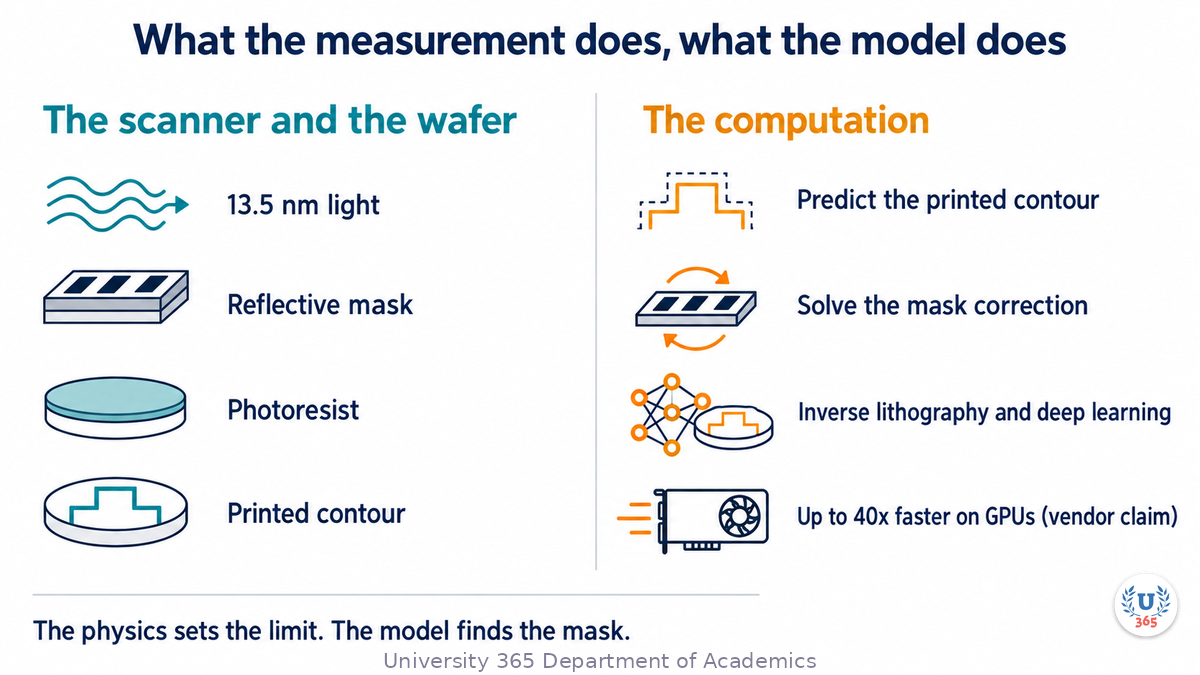
The task where models do real work in this process is not the exposure itself but the calculation that comes before it. Before a mask is written, the pattern is corrected for diffraction: the shapes on the mask are distorted so that the light, after it scatters, prints the intended contour in the resist. That calculation, computational lithography, runs optical proximity correction and inverse lithography technology, and NVIDIA estimated in 2023 that it consumed tens of billions of CPU hours a year. On 21 March 2023 NVIDIA announced cuLitho, a library that runs those solvers on GPUs. The company reported up to 40 times the throughput of its CPU baseline, with 500 DGX H100 systems doing the work of 40,000 CPU systems, and said a mask that took two weeks could be processed overnight. TSMC chief executive C.C. Wei said the speed let TSMC deploy inverse lithography and deep learning more broadly in manufacturing.
Treat those figures as a vendor benchmark from 2023, not a measurement you can audit: the baseline is NVIDIA's own configuration, and the claim is about computation, not about the printed wafer. What matters for you is the split. The scanner and the resist set the physical limit; the model finds a mask that reaches it. So when a chip announcement claims a density gain, ask whether it came from a new scanner, a new process step or a better mask calculation, because the three have different costs and different suppliers. And when someone says a model can design a chip, ask which step it changed and what error it was scored on.
How a Chip Is Made
The Five-Minute Version
A chip is a single crystal of silicon with hundreds of layers built on top. The crystal is grown by dipping a seed into molten silicon and pulling it up, then sliced into wafers 300 millimetres across and 775 micrometres thick.
The layers are made by repetition, not by assembly. Coat the wafer with resist, expose it through a mask, wash away the resist that changed, etch the pattern into the layer below with plasma, strip the resist, deposit the next film, and start again. Dope the silicon where it needs to conduct differently, and build copper wires in trenches because copper cannot be etched cleanly.
The number that decides the difficulty is not the transistor size but the layer count. A 28 nm process needs 40 to 50 mask layers, a 7 nm process needs 80 to 85, and a leading-edge logic process runs 600 to 1,000 steps or more. At one to one and a half days per layer, the calendar follows the count.
The light is the second limit. DUV at 193 nm forced multi-patterning, and EUV at 13.5 nm removed some of those passes, at the cost of a vacuum, reflective mirrors with sub-nanometre figure error and a tin plasma at nearly 220,000 degrees Celsius. ASML sells the scanners, ZEISS makes the optics, and no second supplier exists.
The caveat is that all of this describes capability, not profit. Node names no longer measure a feature, density gains increasingly come from packaging and design, and the public sources do not report yield or cost per transistor. The money is concentrated: 135.1 billion dollars of equipment billed in 2025, 79 per cent of it in three countries.

How a Chip Is Made
Sources
All sources below were opened and read on 22 October 2026.
ASML product page ASML, EUV lithography systems, including the NXE and EXE generations (accessed 22 October 2026)
ZEISS on the light source ZEISS SMT, EUV lithography: the light behind the digital age (accessed 22 October 2026)
IEEE Spectrum on EUV IEEE Spectrum, EUV Lithography Finally Ready for Chip Manufacturing (5 January 2018)
Equipment billings SEAJ and SEMI, World Wide SEMS Report, semiconductor equipment billings 2025 (8 April 2026)
Cycle time and layer counts Semiconductor Engineering, Battling Fab Cycle Times (2017)
Copper metallisation Cheng, Lee and Huang, Copper Metal for Semiconductor Interconnects, IntechOpen (26 January 2018)
Wafer specification Silicon Valley Microelectronics, 300 mm Silicon Wafer datasheet SV025
Polysilicon purification Bernreuter Research, Polysilicon Production: Siemens Process (accessed 22 October 2026)
Computational lithography NVIDIA, NVIDIA, ASML, TSMC and Synopsys Set Foundation for Next-Generation Chip Manufacturing (21 March 2023)


Comments